


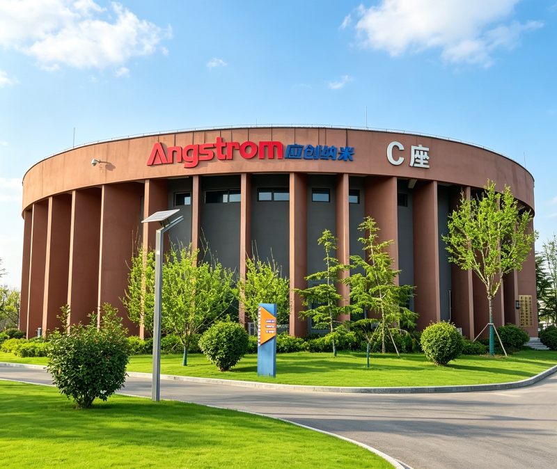
ABOUT US
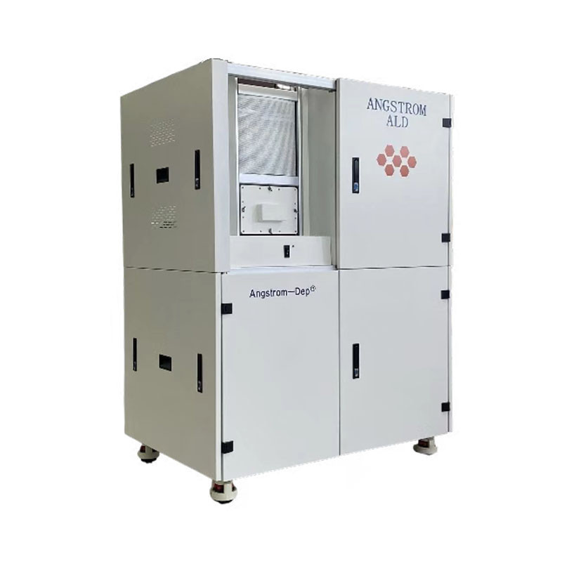
● The Angstrom-dep ® atomic layer deposition (ALD) system was launched by Emmi Thin Film Technology Corporation of the United States.
● Among the company's technical staff are members of the National Academy of Engineering of the United States, researchers from US national laboratories, and committee members of the International Semiconductor Technology Development Map (ITRS) in the fields of plasma and thin films
● The company is one of the earliest in the world to introduce a commercial ALD system with powder ALD functionality. It has close cooperation with US national laboratories and many universities in the fields of using thermal ALD and plasma ALD for nanoparticle modification and performance regulation of nanopporous materials, and has won the R&D100 International Award in 2011 and 2015.
0
+
Support customization
0
%
After-sales guarantee
Nano-scale fabrication of <s:1> metal electrodes (TiN, Ru) and interlinked structures (Cu, TaN);
<s:1> Surface coating of MEMS devices, enhancing wear resistance and stability.
Catalyst carrier modification (such as Pt/Al₂O₃) enhances the utilization rate of active sites and anti-poisoning ability.
Transparent conductive films (ZnO:Al, ITO), suitable for flexible electronic devices.
Antibacterial films (such as Ag-doped oxides) are applied in medical consumables.
TECHNICAL FEATURES
The Angstrom ALD system takes high precision, high uniformity and wide material compatibility as its core advantages. The key technical parameters are as follows
Thickness control: Single-atom layer precision, precisely regulating the film thickness through the number of cycles (growth <1 nm per cycle).
Temperature range: Substrate heating temperature 25℃ to 450℃ (optional up to 650℃), compatible with low-temperature deposition requirements (such as biomedical coatings).

Sedimentary performance
Angstrom ALD
Precursor compatibility: 4, 6, or 8 selectable precursor source paths are available, with a source bottle capacity of 100cc. It supports temperature control from room temperature to 250℃ and is compatible with the deposition of materials such as oxides (Al₂O₃, HfO₂), nitrides (TiN, AlN), and metals (Pt, Cu).
Vacuum and carrier gas: Standard Alcatel mechanical pump, molecular pump or dry pump is available as options; The carrier gas supports nitrogen/argon to ensure the cleanliness of the reaction chamber.
Automation and Integration: Compatible with 100-level cleanroom environments, supports batch processing of multiple wafers (4 to 12 inches), compact equipment size (e.g. 950mm×700mm)

System configuration
Angstrom ALD
Oxides: Al₂O₃, TiO₂, HfO₂, ZnO, etc.
Nitrides: TiN, AlN, TaN, etc.
Metallic elements: Pt, Ru, Cu, Ni, etc.
Composite structure: gradient materials or doped systems such as AlTiNx and HfSiOx.

Material deposition range
Angstrom ALD
MATERIAL DIVERSITY
By self-limiting surface reactions, single-atom layer thickness regulation is achieved, with a film thickness error of less than 0.1nm.

Atomic-level precision control
Technical advantage
The coverage uniformity of complex 3D structures (such as nanoporous holes and high aspect ratio steps) is over 95%, solving the "shadow effect" problem of traditional technologies.

Excellent conformability
Technical advantage
Supports nearly a hundred materials such as oxides, nitrides, metals, sulfides, etc., and can customize multi-component composite films (such as gradient alloys, doped systems).

Material diversity
Technical advantage
The minimum deposition temperature can reach room temperature, making it suitable for heat-sensitive substrates such as polymers and biomaterials.

Low-temperature process compatibility
Technical advantage
It supports batch processing of large-sized wafers ranging from 8 to 12 inches and is compatible with the automated processes of semiconductor production lines. It has been adopted by research institutions such as the Institute of Chemistry, Chinese Academy of Sciences, Peking University, and University of Electronic Science and Technology of China.

Industrial adaptability
Technical advantage
OUR BLOG & NEWS


GET IN TOUCH